
Overview of Digital design methodology, Representations of Digital Design and understanding of digital systems, logic gates, combinational and sequential logic. Review HDL’s and RTL implementation of digital logic systems.
Introduction to semiconductor technologies, logic gates, Review CMOS basics, CMOS digital design concepts. Understanding CMOS process parameters and characterization of logic gates
Overview of ASIC/SOC design flow, Digital Design Concepts and Physical Design flow setup. Review of ASIC fundamentals & fabrication methodologies.
a) Introduction to digital design
b) Number representation, complements and Boolean logic
c) Basic logic gates and logic functions
d) Optimization techniques for logic functions
e) Design of combinational circuits.
f) Implementation and analysis of combinational circuits like, adders, comparator, multiplier etc.
g) Design of synchronous sequential circuits.
h) Implementation and analysis of sequential circuits Flip-Flops, registers, counters, and simple processor
i) Design of Asynchronous Sequential Circuits
j) Design of Finite State Machines (FSM)
k) Discussion - Special circuits like LFSR, FIFO, barrel shifter etc.
l) Case study – PROTOCOLS LIKE AHB, APB, PCI, UART etc.
a) Introduction to Verilog HDL.
b) Gate-Level modeling.
c) Dataflow modeling.
d) Operators.
e) Data types.
f) Modeling timing and delays.
g) Behavioral modeling.
h) Parameters, tasks and functions.
i) Compiler directives.
j) System tasks.
k) File input/output.
l) Switch-level modeling.
m) User Defined Primitives.
n) Design examples – FSM, ALU, RAM, ROM, UART, Traffic light signal.
a) Introduction to ASIC's and ASIC flows
b) Insight into various ASIC design Architecture
c) Writing RTL for ASIC design flow
d) ASIC Design Flow using Synopsys and cadence Tools
e) Using special digital modules in ASIC design
f) Static RAM and Dynamic RAM
g) Clock and Reset managements, power sequencing
h) Clock gating and low power designs
i) Dedicated arithmetic functions
a) Simulation and synthesis issues.
b) RTL design strategies.
c) Static timing analysis.
a) Introduction to STA
b) Comparison with DTA
c) Timing Path and Constraints
d) Different types of clocks
e) Clock domain and Variations
f) Clock Distribution Networks
g) How to fix timing failure
h) Introductions to timing static and dynamic hazards,
i) Path delay, Gate delay, Metastability states.
j) Sequential timing delays like set-up time, hold time,
k) Maximum frequency, violations, slew, slack.
l) Delay analysis
m) Sequential logic pad to set up,
n) pad to pad,
o) clk to next Reg,
p) Reg to o/p and
q) Reg to Reg. violations wrt sequential circuit.
Design data preparation, process technologies and standard cell libraries. Understanding of standard cell technology parameters, netlist generation and technology mapping. Reviewing timing constraints and IO constraints. Low power and low area design concepts
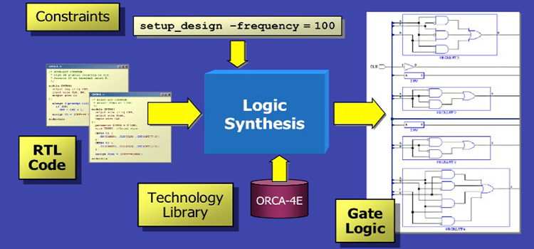
Implementation of RTL design and synthesis, generating netlist and estimating performance of synthesized design. Area/timing report checks, design constraints for synthesis. Efficient synthesis techniques. SDF generation
a) IP synthesis &: Static timing analysis
b) Full chip SoC Static timing analysis
Trainer’s Name
Praveen KumarCourse Fee
:Available Seats
:Schedule
Regular & Weekend Batches
Excellent training provided in Synthesis & STA, Thanks to Neoschip for helping to get my dreamjob

Best training center in Bangalore for VLSI, I have taken synthesis & STA training which helped to get into my dream job
Murthy K
Very good institute for learning vlsi design synthesis & STA, this course helped me to learn from basics to full chip implementation.